- 您现在的位置:买卖IC网 > Sheet目录1992 > CY28446LFXC (Silicon Laboratories Inc)IC CLOCK CALISTOGA CK410M 64QFN
CY28446
.......................Document #: 001-00168 Rev *F Page 8 of 19
.
The CY28446 requires a Parallel Resonance Crystal. Substi-
tuting a series resonance crystal causes the CY28446 to
operate at the wrong frequency and violate the ppm specifi-
cation. For most applications there is a 300-ppm frequency
shift between series and parallel crystals due to incorrect
loading
Crystal Loading
Crystal loading plays a critical role in achieving low ppm perfor-
mance. To realize low ppm performance, use the total capac-
itance the crystal sees to calculate the appropriate capacitive
loading (CL).
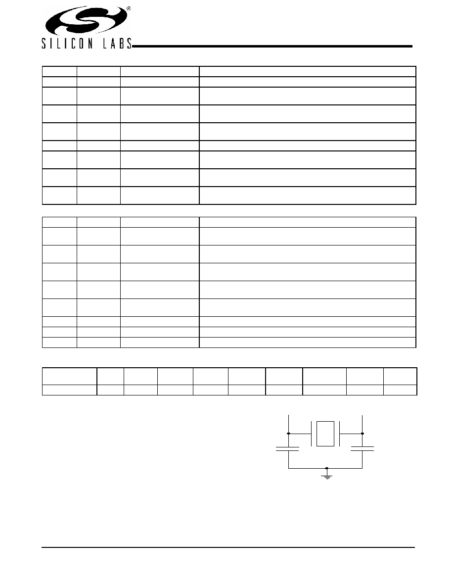
Figure 1 shows a typical crystal configuration using the two
trim capacitors. It is important that the trim capacitors are in
series with the crystal. It is not true that load capacitors are in
parallel with the crystal and are approximately equal to the
load capacitance of the crystal.
.
Calculating Load Capacitors
In addition to the standard external trim capacitors, consider
the trace capacitance and pin capacitance to calculate the
crystal loading correctly. Again, the capacitance on each side
Byte 8: Control Register 7
Bit
@Pup
Name
Description
7
0
Reserved
Reserved set to 0
6
1
SRC[T/C]10
SRC[T/C]10 Output Enable
0 = Disable (Tri-state), 1 = Enable
5
1
SRC[T/C]9
SRC[T/C]9 Output Enable
0 = Disable (Tri-state), 1 = Enable
4
1
SRC[T/C]8
SRC[T/C]8 Output Enable
0 = Disable (Tri-state), 1 = Enable
3
0
Reserved
Reserved set to 0
2
0
SRC10
Allow control of SRC[T/C]10 with assertion of OEA#
0 = Free running, 1 = Stopped with OEA#
1
0
SRC9
Allow control of SRC[T/C]9 with assertion of OEB#
0 = Free running, 1 = Stopped with OEB#
0
SRC8
Allow control of SRC[T/C]8 with assertion of OEA#
0 = Free running, 1 = Stopped with OEA#
Byte 9: Control Register 8
Bit
@Pup
Name
Description
7
0
PCI3
33-MHz Output drive strength
0 = Low, 1 = High
6
0
PCI2
33-MHz Output drive strength
0 = Low, 1 = High
5
0
PCI1
33-MHz Output drive strength
0 = Low, 1 = High
4
0
PCI0
33-MHz Output drive strength
0 = Low, 1 = High
3
0
PCIF0
33-MHz Output drive strength
0 = Low, 1 = High
2
1
Reserved
Reserved set to 1
1
Reserved
Reserved set to 1
0
1
Reserved
Reserved set to 1
Crystal Recommendations
Frequency
(Fund)
Cut
Loading
Load Cap
Drive
(max.)
Shunt Cap
(max.)
Motional
(max.)
Tolerance
(max.)
Stability
(max.)
Aging
(max.)
14.31818 MHz
AT
Parallel
20 pF
0.1 mW
5 pF
0.016 pF
35 ppm
30 ppm
5 ppm
Figure 1. Crystal Capacitive Clarification
发布紧急采购,3分钟左右您将得到回复。
相关PDF资料
CY28447LFXC
IC CLOCK CALISTOGA CK410M 72QFN
CY28547LFXCT
IC CLOCK CK505/410M INTEL 72QFN
CY28548ZXC
IC CLK CK505 960M/965M 64TSSOP
CY28551LFXC-3T
IC CLOCK INTEL/AMD SIS VIA 56QFN
CY28551LFXC
IC CLOCK INTEL/AMD SIS VIA 64QFN
CY2SSTV855ZXI
IC CLOCK DIFFDRV PLL DDR 28TSSOP
CY2SSTV857ZXI-27
IC CLK DDR266/333BUF1:10 48TSSOP
CY2SSTV857ZXI-32
IC CLK DDR266/333BUF1:10 48TSSOP
相关代理商/技术参数
CY28446LFXCT
功能描述:时钟发生器及支持产品 Calistoga RoHS:否 制造商:Silicon Labs 类型:Clock Generators 最大输入频率:14.318 MHz 最大输出频率:166 MHz 输出端数量:16 占空比 - 最大:55 % 工作电源电压:3.3 V 工作电源电流:1 mA 最大工作温度:+ 85 C 安装风格:SMD/SMT 封装 / 箱体:QFN-56
CY28447
制造商:SPECTRALINEAR 制造商全称:SPECTRALINEAR 功能描述:Clock Generator for Intel㈢ Calistoga Chipset
CY28447LFXC
功能描述:时钟发生器及支持产品 Calistoga System Clk Extra SRC Output RoHS:否 制造商:Silicon Labs 类型:Clock Generators 最大输入频率:14.318 MHz 最大输出频率:166 MHz 输出端数量:16 占空比 - 最大:55 % 工作电源电压:3.3 V 工作电源电流:1 mA 最大工作温度:+ 85 C 安装风格:SMD/SMT 封装 / 箱体:QFN-56
CY28447LFXCT
功能描述:时钟发生器及支持产品 Calistoga System Clk Extra SRC Output RoHS:否 制造商:Silicon Labs 类型:Clock Generators 最大输入频率:14.318 MHz 最大输出频率:166 MHz 输出端数量:16 占空比 - 最大:55 % 工作电源电压:3.3 V 工作电源电流:1 mA 最大工作温度:+ 85 C 安装风格:SMD/SMT 封装 / 箱体:QFN-56
CY28506OC
制造商:Rochester Electronics LLC 功能描述:FTG FOR MOTHERBOARDS - Bulk
CY28506OCT
制造商:Rochester Electronics LLC 功能描述:CLOC - Tape and Reel
CY28507ZC-3
功能描述:时钟缓冲器 PacketClockClk RoHS:否 制造商:Texas Instruments 输出端数量:5 最大输入频率:40 MHz 传播延迟(最大值): 电源电压-最大:3.45 V 电源电压-最小:2.375 V 最大功率耗散: 最大工作温度:+ 85 C 最小工作温度:- 40 C 封装 / 箱体:LLP-24 封装:Reel
CY28508OCT
制造商:Cypress Semiconductor 功能描述: